
Conductive layers are essential for your electronic devices because they guarantee proper electrical flow, preventing overheating and power loss. They often work behind the scenes, but even small variations can cause big issues like device failure or reduced lifespan. Choosing the right materials and manufacturing techniques is key to durability and performance. If you want to understand how these hidden layers keep your devices working smoothly, there’s more to explore.
Key Takeaways
- Conductive layers enable efficient electrical current flow, directly impacting device performance and longevity.
- Variations in material quality or compatibility can cause failures, even if the layers are hidden.
- Manufacturing precision ensures uniform conductivity, preventing defects like delamination or overheating.
- Small improvements or issues in conductive layers can significantly influence overall device reliability.
- Proper material selection and process control are vital for preventing costly electronic device failures.

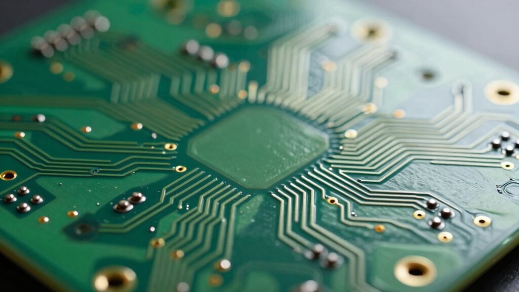
Conductive layers are a pivotal component in many electronic devices, directly impacting their performance and reliability. These thin films or coatings facilitate the flow of electrical current, making them essential for everything from circuit boards to sensors. Their importance often goes unnoticed because they operate behind the scenes, but a slight variation in their quality can cause significant issues. When you understand their role, you’ll see why selecting the right conductive layer matters more than most people realize.
Conductive layers are hidden yet vital, ensuring device performance and reliability through precise material choice and manufacturing.
At the core, electrical conductivity determines how efficiently these layers transmit current. If the conductive layer isn’t tailored for high electrical conductivity, your device might experience increased resistance, leading to overheating, power loss, or even failure. This is why material selection is essential. Different materials—like copper, silver, or conductive polymers—offer varying levels of electrical conductivity. Choosing a material compatible with your device’s environment, operating temperature, and electrical requirements guarantees the best performance. Material compatibility isn’t just about selecting a good conductor; it’s about ensuring that the layer interacts seamlessly with other components without causing corrosion, delamination, or degradation over time.
You might think that any conductive material would do, but that’s far from the truth. The wrong material can lead to issues such as poor adhesion, increased electrical resistance, or incompatible thermal expansion, all of which compromise device integrity. For example, if the conductive layer isn’t compatible with the substrate material, it may peel or crack under stress, risking device failure. That’s why understanding the interplay between electrical conductivity and material compatibility is essential when designing or repairing electronic components. Additionally, the manufacturing process used can significantly influence the quality and durability of the conductive layer. Proper control of deposition techniques can help achieve uniform, high-quality coatings that withstand operational stresses. A thorough understanding of material properties can help in selecting the most suitable materials for specific applications, ensuring long-term performance. Moreover, manufacturing parameters such as temperature, pressure, and environment can greatly affect the final quality of the conductive layer, emphasizing the need for precise control during production.
Furthermore, the manufacturing process influences the effectiveness of conductive layers. Techniques like sputtering, electroplating, or printing need to be compatible with the chosen material to produce uniform, defect-free layers. A poorly applied layer—even if made from the best material—can suffer from uneven conductivity or delamination, reducing device reliability. This highlights how important it is to match manufacturing processes with the properties of the materials you select.
In essence, the significance of conductive layers extends beyond their basic function. They are a fundamental factor in ensuring your electronic devices operate efficiently, last longer, and perform reliably. By paying close attention to electrical conductivity and material compatibility, you can prevent costly failures and maximize device performance. These layers might be small and hidden, but their impact on your devices’ health and functionality is anything but minor.

Zehhe Copper Foil Tape with Double-Sided Conductive (1/4inch X 21.8yards)- EMI Shielding,Stained Glass,Soldering,Electrical Repairs,Slug Repellent,Paper Circuits,Grounding (1/4inch)
[CONDUCTIVE ADHESIVE] – Double-sided Conductive means both sides of this tape will carry current so whether it's soldering,…
As an affiliate, we earn on qualifying purchases.
As an affiliate, we earn on qualifying purchases.
Frequently Asked Questions
How Do Conductive Layers Affect Device Durability?
Conductive layers greatly impact your device’s durability through material conductivity and layer thickness. If the layer is too thin, it may crack or wear out quickly, reducing conductivity and risking failure. Conversely, a carefully determined layer thickness ensures reliable electrical flow and better resistance to environmental stress. Choosing the right material conductivity and suitable layer thickness helps your device withstand daily use, extending its lifespan and maintaining performance over time.
Can Conductive Layers Be Recycled or Reused Effectively?
Think of conductive layers as treasure chests—valuable but tricky to open again. Recycling challenges often hinder their reuse, as delicate materials need careful handling. While some conductive layers can be recycled or reused effectively, the process isn’t always straightforward. You’ll find that reuse potential depends on material quality and recycling tech. With advancements, you could see more sustainable options emerge, turning these layers into reusable assets rather than discarded waste.
What Environmental Factors Impact Conductive Layer Performance?
Environmental factors like environmental degradation and material stability drastically impact conductive layer performance. You’ll notice that exposure to moisture, temperature fluctuations, and pollutants can deteriorate the conductive materials over time. These conditions cause corrosion or corrosion-related failures, reducing efficiency. Maintaining stable environmental conditions and selecting materials resistant to degradation help guarantee the longevity and reliability of conductive layers, especially in challenging environments.
Are There Health Risks Associated With Conductive Layer Materials?
You might worry about health risks from conductive layer materials, but most are safe if chosen carefully. While material toxicity can be a concern, reputable manufacturers ensure long-term stability and safety standards. When properly tested and certified, these materials pose minimal health risks. So, there’s no need to *guarantee* health issues—just select high-quality, certified conductive layers, and you’ll enjoy their benefits without worry.
How Do Conductive Layers Influence Overall Device Weight and Flexibility?
Conductive layers impact your device’s weight and flexibility mainly through their thickness and material conductivity. Thicker layers add weight and reduce flexibility, making devices stiffer and bulkier. High conductivity materials can achieve efficient performance with thinner layers, saving weight and enhancing flexibility. By choosing best conductive layer thickness and materials, you can enjoy a lighter, more flexible device that still delivers reliable electrical performance.

KINGTAIXI Nadhesive Paint Pen,0.7ml Conductive Silver Paste, Adhesive Paint Pen for Keyboard PCB Repair and Electronics Repair Applications
Core Advantages: Our Silver Conductive Paint offers exceptional electromagnetic shielding performance exceeding 80dB, ensuring reliable protection for your…
As an affiliate, we earn on qualifying purchases.
As an affiliate, we earn on qualifying purchases.
Conclusion
In the end, understanding the importance of conductive layers can truly transform your approach to electronics. Imagine designing a wearable health device that seamlessly tracks your crucial signs; without proper conductive layers, signals might fail or become inaccurate. By prioritizing these layers, you guarantee reliability and performance. So next time you build or troubleshoot, remember — conductive layers aren’t just a detail, they’re the backbone of effective, functional technology.

Conductive Polymers and Their Composites
As an affiliate, we earn on qualifying purchases.
As an affiliate, we earn on qualifying purchases.
PCB Trace Repair Kit Soldering Lugs Solder Piece Rework Pad, Circuit Board Repair Kit, Repairs Spots Welding Point Mat for Phone IC Touch PCB Fingerprint Welding Plate with Copper Wire Design
COMPLETE PACKAGE: Our pcb trace repair kit includes 2780 pieces of soldering pads, solder blocks, and solder pad…
As an affiliate, we earn on qualifying purchases.
As an affiliate, we earn on qualifying purchases.